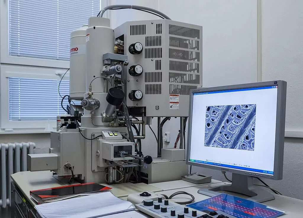
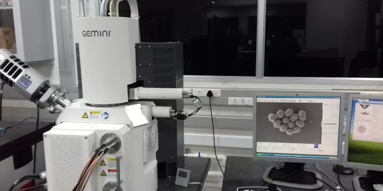
Scanning Electron Microscopy (SEM) is a powerful imaging tool that can reveal extremely small details of materials at high magnifications with excellent clarity and depth of field. It differs from optical microscopes because it uses electrons to create images, not light.
An SEM creates images by scanning a focused beam of electrons across a sample’s surface. By revealing information on a material’s surface composition and topography. The rastering action of the beam stimulates backscattered electrons and secondary electrons.
What is Scanning Electron Microscopy?

Scanning Electron Microscopy (SEM) is a powerful and versatile analytical technique used for many applications. It produces high-resolution, detailed images of the surface of a sample and can reveal information about its composition and topography.
Using an SEM service, like those offered by microvisionlabs.com, images are created using a focused electron beam rather than light, allowing you to see fine features of a sample at high magnifications with clear images and a substantial depth field. SEMs are a vital tool for many different sectors and industries. It is because of their capacity to provide finely detailed, three-dimensional images.
The electron beam is created at the top of the microscope by an electron gun that fires a beam of electrons. Through an array of lenses that focus the beam down to a very tiny spot on the sample. This beam interacts with atoms on the sample’s surface and a limited sub-surface volume. It then generates various signals collected by detectors. These include backscattered electrons (BSE) and secondary electrons (SE).
How Does Scanning Electron Microscopy Work?
It has many different applications in the fields of aerospace, chemistry, energy, and electronics. The instrument operates by accelerating electrons to high energies and then scattering them off the surface of a sample. The electron beam is narrowed down to a diameter of about 0.4 to 5nm by one or two condenser lenses and then deflected in the x and y axes using scanning coils or deflector plates.
When the electron beam interacts with a solid sample. It loses energy by random scattering and absorption within a teardrop-shaped sample volume known as the interaction volume. This energy loss is reflected as secondary and backscattered electrons (BSE). It is then diffracted backscattered electrons (EBSD) and photons, characteristic X-rays, visible light, and heat.
What are the Benefits of Scanning Electron Microscopy?
Scanning Electron Microscopy (SEM) is a powerful materials analysis technique that creates incredibly detailed images of your sample. It can magnify an image up to 2 million times and captures information about how a sample interacts with the electron beam.
A scanning microscope uses an electron gun to generate a beam of energetic electrons. It then travels down the microscope’s column and onto a series of electromagnetic lenses. The condenser lens controls the size of the electron beam, while the objective lens focuses it onto a very small spot on the sample.
The electrons pass through the lens to the detector, picking up information and processing it. This allows you to see detailed three-dimensional and topographical imaging of the surface of your sample.
SEM is important because it allows scientists and researchers to examine the fine details of a sample’s surface at a very high magnification and resolution. Typically ranging from a few nanometers to several micrometres. This enables the study of the microstructure and composition of materials. Such as metals, semiconductors, polymers, and biological samples, at a level of detail that is not possible with other types of microscopy.
SEM has numerous applications in various fields, including materials science, biology, chemistry, geology, and forensic science. It is used to study the structure and properties of materials and investigate the surface morphology and topography of biological specimens. Also, to analyze the composition and distribution of elements in a sample.
What is the Cost of Scanning Electron Microscopy?
The purchase of an electron microscope is a high upfront cost. They also have unstated expenses that, over time, could total thousands or even millions of dollars. Companies like CAE Marketing & Consulting can increase this service’s website and target customers that would most likely need lab microscopy services.
The cost of scanning electron microscopy varies depending on many factors, including the type of SEM and its specifications. It is important to consider what you need to achieve with your SEM and the amount of detail you want to see.
For example, a typical SEM will use a tungsten source to emit an electron beam that is focused and directed at the sample. It also uses a series of lenses and apertures to control the beam’s speed.
The resolving power of SEMs is much higher than that of light microscopes. This allows users to see details down to the atomic level.

